


See you at the next stop in Wuhan
Release time:
Mar 26,2024
CHENG FENG
珠海诚锋电子科技有限公司
On April 8-11, 2024, the annual compound semiconductor industry event——
The 2024 Jiufengshan Forum and China International Compound Semiconductor Industry Expo (JFSC&CSE) will be held at the Wuhan Optics Valley Technology Exhibition Center.
Zhuhai Chengfeng Electronic Technology Co., Ltd. will present its new products at this grand event and sincerely invite industry colleagues to visit booth 2T43 for exchange and cooperation.

Welcome!
JFSC&CSE 2024
Dear industry colleagues: Hello!
Chengfeng Technology sincerely invites you to participate in the "2024 Jiufengshan Forum and China International Compound Semiconductor Industry Expo" held at the Wuhan Optics Valley Technology Exhibition Center in Hubei from April 9th to 11th. The company will bring core products and the latest solutions to booth 2T43, waiting for friends from all walks of life to visit and negotiate.
On April 9th, Wuhan Optics Valley, see you and never part!
About Chengfeng Technology

Zhuhai Chengfeng Electronic Technology Co., Ltd., headquartered in Zhuhai, the core city on the west bank of the the Pearl River Estuary in the Dawan District, has set up branches and offices in Suzhou, Hefei, Shanghai, Beijing, Shenzhen, Chengdu, Wuhan, Xiamen, Shaoxing, Thailand, Singapore and other places at home and abroad to set foot in China and look around the world.
For many years, we have been focusing on the semiconductor optical visual inspection equipment industry and are a semiconductor visual inspection equipment manufacturer that integrates research and development, production, and sales. The company has gathered a group of elite talents who have been deeply involved in the field of machine vision technology for more than 20 years. They have independently developed various high sensitivity and low noise light source optical path technologies, as well as various software detection algorithms and machine learning algorithms. Each electronic component has been strictly selected and only legitimate brands are used. The machining accuracy of the entire machine meets international standards, creating semiconductor equipment with completely independent intellectual property rights, and providing customers with comprehensive semiconductor manufacturing yield control and visual defect detection solutions.
Chengfeng Technology focuses on the research and development of FAB graphic wafer detection equipment. By combining years of accumulated machine vision technology, profound optical path design achievements, and intelligent software detection algorithms with the latest process requirements in the industry, we have designed a series of graphic wafer detection equipment with complete intellectual property rights, suitable for the CFW920 series/CFW820 series for front-end process control, the CFW380 series for back-end process detection, and the CFW680 series for infrared detection. Chengfeng Technology continues to innovate and benchmark against global leading technologies. We develop and provide process control and process promotion solutions to support the development of multiple cutting-edge fields such as optical communication and new energy.
Chengfeng Technology, with its outstanding testing capabilities and excellent service quality, efficiently meets customer needs, and hands over the power of evaluating equipment quality to customers, making them truly gods. The company has obtained more than 40 national patent technology certificates, and has been awarded certification qualifications such as National High tech Enterprise, Specialized and Innovative Enterprise, ISO-9001 Quality Management System, ISO-14001 Environmental Management System, and Intellectual Property Management System.
Chengfeng Technology, with continuous innovation, drives value growth through innovation, enhances brand value through quality, and is committed to solving the bottleneck problem of domestic semiconductor visual inspection, truly achieving domestic substitution, and becoming a leader in visual inspection equipment in the semiconductor industry.
Partial product introduction
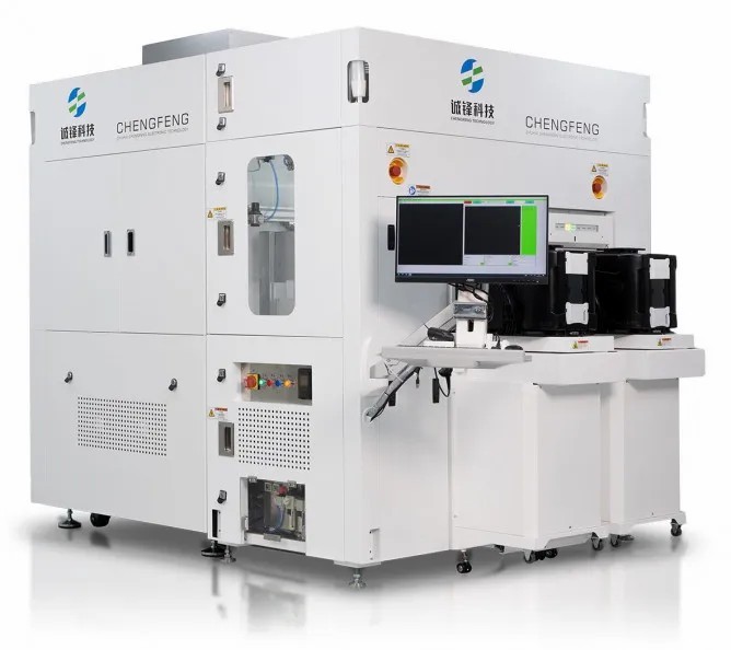
Product Name: CFW920-Fab Front Process Control Equipment
Application scenario: ADI/AEI/Post CMP/Advanced Packaging/Cutting Path/0QC
Applicable fields:
1. FAB front-end process control
2. Supports 12 "/8"/6 "wafer
3. Support Taiko/Shin thinning process
4. Support wafer flipping function
5. ADC automatic defect classification
Pixel resolution: 170 nm@20X
Magnification: 2X/5X/10X/20X, 50X/100X
Features: yield control, fine defect detection

Product Name: CFW820-Fab Front Defect Detection Equipment
Application scenario: ADI/AEI/Post CMP/Advanced Packaging/Cutting Path/0QC
Applicable fields:
1. FAB front-end process control
2. Supports 12 "/8"/6 "wafer
3. Support Taiko/Shin thinning process
4. Support wafer flipping function
5. ADC automatic defect classification
Pixel resolution: 976nm@5X
Magnification ratio: 2X/5X/10X/20X
Features: AOI, rapid screening of major defects

Product name: CFW380 Fab rear section defect detection
Application scenarios: OQC/detection after cutting/detection after film expansion
Applicable fields:
1. FAB quality final inspection
2. Detection after wafer slicing/film expansion
3. Supports 12 "/8"/6 "wafer
4. Support Taiko/Shin thinning process
5. Support wafer flipping function
6. ADC automatic defect classification
Pixel resolution: 2.4 μ M @ 2X
Magnification: 1x/2X/5X
Features: yield control, fine defect detection
Parallel Forum 2: Core Equipment of Compound Semiconductors
Time: 08:30-18:00 on April 10th, 2024&08:30-12:00 on April 11th, 2024
Location: Wuhan Optics Valley Technology Exhibition Center • Third Floor, China
Reporting guests:

Longfengcai
Product Director of Zhuhai Chengfeng Electronic Technology Co., Ltd
Longfengcai,I graduated from the Department of Computer Science and Technology at Nanjing University of Posts and Telecommunications with a bachelor's degree. I have over 20 years of experience in software and algorithm development, as well as team management. I have extensive experience in embedded software system development and technical team management, as well as years of experience in visual software algorithm development for semiconductor optical testing equipment. I also have experience in cross industry product management and extensive experience in multinational enterprise cooperation.
Report title:
"Application of dedicated optical denoising technology in wafer AOI"
Report Summary:
1) The advantages of Chengfeng optical noise reduction technology
2) Introduction to Application Cases of Chengfeng Optical Noise Reduction Technology
3) Chengfeng wafer AOI product introduction
Contact information:
Enterprise Name: Zhuhai Chengfeng Electronic Technology Co., Ltd
Enterprise official website: www.klat.com. cn
Contact person: Pan Lina
Contact phone number: 13168691510
Email: panlina@chengfengvs.com
Company address: Building 4, No.1 Keji 7th Road, High tech Zone, Zhuhai City, Guangdong Province

Previous Page
Previous Page
NEWS
Company address: Building 4, Zhongdian High tech Industrial Park, Keji 7th Road, Tangjiawan Town, High tech Zone, Zhuhai City, Guangdong Province
Company address: Wanlong Building, No. 29 Xinfa Road, Suzhou Industrial Park, Suzhou City, Jiangsu Province
Company address:Comprehensive Protection Building at the Intersection of Dongfang Avenue and Dayu Road in Xinzhan District, Hefei City, Anhui Province
Company address: Building 1, Investment Promotion High tech Network Valley, Donghu High tech Zone, Wuhan City, Hubei Province
Stay Connected
Copyright © 2022 Zhuhai Chengfeng Electronic Technology Co., Ltd.