


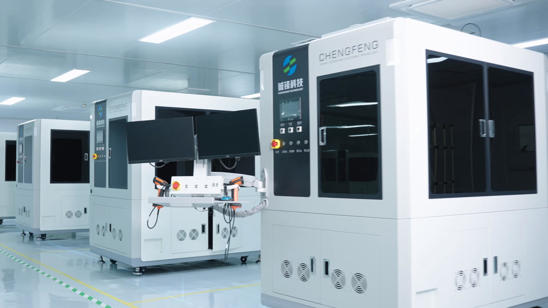
CFW920 nanometer graphics wafer testing equipment , Wafer Type: Bare, Taiko, Thin , Application: ADI/AEI/Post CMP/ Advanced Packaging/Cutting Path , Application field: FAB front process control Product features: yield control, small defect sampling
View More > >
Passive Component Inspecting Equipment
The hexahedral appearance detection and sorting equipment can eliminate the wrong detection and missing detection caused by fatigue in eye detection by self-developed algorithm. The system parameter setting is simple and the detection specifications are unified. It can quickly and accurately identify all kinds of small defects on the surface of all kinds of fine products. Using ultra-high resolution cameras imported from Germany and self-developed high-precision algorithms, according to customer needs, it can realize fine material detection of various shapes, accurately detect a variety of surface defects of products, with accuracy up to pixel level, and at the same time, it can achieve positive and negative recognition, classification and other functions.
View More > >
Lead Frame Inspecting Equipment
The lead frame visual inspection equipment is specially designed for defect detection during the production of chip supports in the semiconductor industry. Optical imaging, image processing, deep learning and automation technologies are applied to meet all kinds of defect detection during the production of chip supports. The company specially sets up a visual inspection solution laboratory, with advanced visual equipment and professional visual team, the detection software and algorithm independent design to solve customers' visual problems as the core, truly achieve one to one visual solution service.
View More > >
Specific parameter Equipment specification ≤0.01% (0 missed detection can be achieved for serious defects) Detection accuracy 200 nanometers ~3 microns Camera configuration 25 million +12 million high speed industrial cameras Detection time Single chip (8mm x 5mm) : ≤0.5 seconds Omission rate ≤0.01% serious defects can achieve 0 missed detection) Core characteristics Chengfeng Wafer AOI CF910 is specially designed for graphic wafer detection. It can detect wafer surface defects including: wafer graphic pattern defects (missing/incomplete/bad size/scratches/foreign bodies, etc.) and random surface defects (broken/dirty/scratches/foreign bodies, etc.). The software adopts the mature algorithm combining Chengfeng Technology AI and traditional vision, which can detect the appearance defects of wafer with high precision and greatly reduce the false positives of defects. Scope of application Optical inspection and calibration of graphic patterns in various wafer manufacturing processes Wafer end of shipment quality inspection Closed test manufacturing defect detection after segmentation and segmentation
View More > >
CFW920 nanometer graphics wafer testing equipment , Wafer Type: Bare, Taiko, Thin , Application: ADI/AEI/Post CMP/ Advanced Packaging/Cutting Path , Application field: FAB front process control Product features: yield control, small defect sampling
View More > >
VARIOUS APPLICATIONS
Appearance defect detection in wafer, chip lead frame, magnetic core, integrated inductor, diode, resistor, capacitor, chip, precision electronic components and other fields.
Chip Lead Frame
Magnetic Core
Wafer
Resistance
Capacitance
Wafer
Crystal Chip
Precision Electronic Components
LED Bracket
Diode
WHY CHOOSE US
Our Factory
More than 7800㎡ of the Factory scale
Quality
Strict quality control on every process.
Technology
Top industrial visual inspection technology
Service
Full cycle service process
Incorporated In
Worldwide
National Patent
Corporate Team
ABOUT US
Zhuhai Chengfeng Electronic Technology Co., LTD., headquartered in Zhuhai, the core city on the west bank of the Pearl River Estuary in the Greater Bay Area, the company has set up branch offices in Suzhou, Hefei, Shanghai, Beijing, Shenzhen, Chengdu, Wuhan, Xiamen, Shaoxing, Chongqing, Thailand, Singapore and other domestic and foreign countries, and the sales scope radiates to the world. Over the years, it has focused on the semiconductor optical vision inspection equipment industry, and is a manufacturer of semiconductor vision inspection equipment integrating research and development, production and sales. The company has gathered a group of elite talents who have been deeply engaged in the field of machine vision technology for more than 20 years, independently developed a variety of high-sensitivity, low-noise light source and light path technologies as well as a variety of software detection algorithms and machine learning algorithms, and has both hardware institutions and electrical technology research and development and production capabilities to create semiconductor equipment with completely independent intellectual property rights. To provide customers with a full range of semiconductor manufacturing yield control and visual defect detection solutions. Chengfeng Technology focuses on the research and development of nanoscale graphics wafer detection equipment, passive component appearance defect detection equipment, lead frame appearance defect detection equipment, combining machine vision technology accumulated over the years, profound optical path design results and intelligent software detection algorithms with the latest process requirements of the industry. A series of graphic wafer inspection equipment with complete intellectual property rights have been designed, which is suitable for the CFW920 series /CFW820 series for the front process control, CFW380 series for the rear process inspection, and CFW680 series for infrared inspection. Chengfeng Technology continues to innovate, constantly benchmarking the world's leading technology, and has applied series of products in many frontier fields such as communications and new energy. Chengfeng Technology with excellent testing ability and excellent service quality, efficient to meet customer needs, has obtained more than 40 national patent technology certificates, won the national high-tech enterprises, specialized special new enterprises, ISO-9001 quality management system, ISO-14001 environmental management system, intellectual property management system certification qualifications. Chengfeng Technology, continuous innovation, with innovation to drive value growth, quality to enhance brand value, is committed to solving the domestic semiconductor visual inspection "jam neck" problem, truly realize the localization of replacement, become the semiconductor industry visual inspection equipment leader.
OUR CLIENTS
The products of Chengfeng Electronics have been recognized and praised by many customers at home and abroad in the industry, and have been exported to the industrial bases of semiconductor industry concentration in Southeast Asia.


LATEST NEWS
Technological innovation service industry to live up to the times hand in hand
2024-04-11
The 2024 Jiufengshan Forum and Compound Semiconductor Industry Expo was successfully concluded at Wuhan Optics Valley Expo Center on April 11. This event is the largest and highest-standard benchmark exhibition in the domestic compound semiconductor field. The Jiufengshan Forum adopts the mode of "one opening conference, eight industry forums, many industry conferences, and many side exhibitions". It will be attended by more than 10 academicians at home and abroad. A total of more than 150 guests will share the industry report. The agenda is quite substantial. Let's review the grand occasion together.
2024 Romantic Wuhan Chengfeng Technology Meet You
2024-04-09
China International Compound Semiconductor Industry Expo opened in Wuhan Optics Valley Science and Technology Exhibition Center. Let's follow the footsteps of Xiaobian and see the scene.
See you at the next stop in Wuhan
2024-03-26
The 2024 Jiufengshan Forum and China International Compound Semiconductor Industry Expo (JFSC&CSE) will be held at the Wuhan Optics Valley Technology Exhibition Center.
From April 9th to 11th, Chengfeng Technology invites you to gather at the CSE Compound Semiconductor Industry Expo and invites industry colleagues to visit booths A2 and 2T43 at the Wuhan Optics Valley Technology Exhibition Center
2024-03-26
On April 8-11, 2024, the annual compound semiconductor industry event - the 2024 Jiufengshan Forum and China International Compound Semiconductor Industry Expo (JFSC&CSE) will be held at the Wuhan Optics Valley Technology Exhibition Center. Zhuhai Chengfeng Electronic Technology Co., Ltd. will present its new products at this grand event and sincerely invite industry colleagues to visit and exchange cooperation at booth 2T43.
KEEP IN TOUCH
Company address: Building 4, Zhongdian High tech Industrial Park, Keji 7th Road, Tangjiawan Town, High tech Zone, Zhuhai City, Guangdong Province
Company address: Wanlong Building, No. 29 Xinfa Road, Suzhou Industrial Park, Suzhou City, Jiangsu Province
Company address:Comprehensive Protection Building at the Intersection of Dongfang Avenue and Dayu Road in Xinzhan District, Hefei City, Anhui Province
Company address: Building 1, Investment Promotion High tech Network Valley, Donghu High tech Zone, Wuhan City, Hubei Province
Stay Connected
Copyright © 2022 Zhuhai Chengfeng Electronic Technology Co., Ltd.